Voltage regulators are available as easy to use three terminal
integrated circuits - one terminal for the input voltage, one for the
output voltage, and one for the ground (0V). The most commonly used are
from the
78XX series - 7812 for 12 Volts, and 7805 for 5 Volts etc. Also of particular use for
renewable energy generators are very efficient
low dropout regulators such as the
LM2940 series - LM2940CT-12 for 12 Volt etc.
One common shortfall of these common regulators is they are rated at just
1 Amp
output current. It is usually possible to use them with higher
currents, but a large heatsink and/or fan is essential. Regulators for
higher currents than 1 Amp are available, but tend to be expensive, and
still require good heatsinking.
Pictured above is a circuit from the
Fairchild LM7812 datasheet. This uses a
power transistor and a
power resistor
to take on some of the workload enabling higher currents to be
regulated. With this set up, the power transistor and power resistor
need
heatsinking, and selecting the correct specification of transistor and resistor, and getting everything set up is not particularly easy.
One alternative is instead to
parallel connect multiple three terminal regulators, with each regulator handling up to 1 Amp of current.
Parallel Connecting Mulitple Voltage Regulators
Voltage regulators such as the LM7812 cannot just be connected in
parallel without additional circuitry. Each voltage regulator, though
nominally rated at the same voltage, will in practice output a slightly
different voltage - for example, three LM7812's could output 11.98,
12.01, and 12.06 respectively.
This tiny difference in voltage has the disastrous consequence of making
the regulator with the lowest output voltage trying to carry
all of the current. This will cause it's internal
thermal protection
to trigger (as the regulator overheats) effectively removing that
regulator from the circuit and kicking off a chain reaction up through
the remaining parallel-connected regulators.
The circuit shown above* (from the
EDN article
High-Current Supply uses Standard Three-terminal Regulator) has two
LM7812 voltage regulators connected in parallel for a maximum total output current of 2 Amps - double the rated current of one LM7812.
*
Diodes D1, D2, and D should be 1N4007 according to the EDN article,
but common 1N4001 diodes will be fine as they are rated up to 50V which
is more than enough. The capacitors are supposed to be C=47,000uF, C1
and C2 are 4,700uF, but as a 47,000uF capactitor is expensive and
physically very large we tested this regulator using a 4,700uF for C,
and 1,000uF for C1 and C2 and had no problems.
An even simpler way to parallel connect multiple voltage regulators together is to add very low (below 1 Ohm)
ballast/
equalising resistors in series with the regulator outputs. Doing so should make the regulators
share current equally and therefore operate together without problems. It is worth noting however that this approach to
load balancing makes the voltage regulation a bit less accurate.
An example of this simplistic approach in use can be seen in the above
experimental 12V 6A power supply* in which six
LM7812 regulators were connected in parallel with
0.25 Ohm
load balancing resistors (made up of four 1 Ohm resistors in parallel)
connected in series with the output from each 7812 regulator. The
schematic shows the key elements in this 6 Amp 12 Volt regulator.
*
The original circuit diagram was published on the Wroclaw
University of Technology website back when we first published this
article in 2006/7. Unfortunately that article is no longer online.
High Current Variable Voltage Regulation
Where you need to have a user variable voltage output, the
LM317
is an excellent adjustable voltage regulator to use. The output voltage
is adjusted using a couple of resistors, and one of these resistors can
be replaced with a
potentiometer to give an adjustable output.
While the LM317T for example is limited to a continuous output of 1-1.5A subject to sufficient heatsinking, one or more
power transistors can be added as shown above to make an adjustable
high current power supply. Click here for full details:
LM317 Adjustable Power Supply.
Comment on this Article
If you have any comments on this article, please email them to
neil@reuk.co.uk.
Hello from Kentucky USA!
In regard to this page, I have drawn up a couple of 78xx high current circuits you might like to consider. I've used them for a 30amp power supply with a 7815 regulator.
REUK Added Info: The MJE3055 is an NPN silicon power transistor rated at up to 60V, up to 75 Watts, and up to 10 Amps. Click here to view the MJE3055 Datasheet for more information.
If
you are unable to find the MJE3055, any NPN power transistor with a
similar rating can be used instead. Click here to view a selection of NPN power transistors.
I have since switched to using the better LM723 regulator so that I can adjust the voltage and it is far more reliable than the 78xx. I have used the LM723 for a 105amp supply.
REUK Added Info:The LM723
is a voltage regulator rated for outputs of 150mA at an adjustable
voltage from 2V to 37V. By adding transistors as shown in the schematics
above high output currents at the regulated voltage can be output.
Click here to view the LM723 datasheet.
The LM723 is available in the UK from around 30 pence. Click here to buy an LM723 now.
I've learned a few things on your site so I thought I'd pass along a little in return.
Ken Weaver, 17th August 2009
The benefit of this first schematic is that the output is actually regulated; the PNP is fully in the feedback loop.
However
in Ken's circuit, the bases of the 3055 are regulated, but not the
emitters, where the output is taken. Thus for every current ratio of 2.7
the voltage drops by 25mV.
Nick, 10th July 2012 |
rrent.
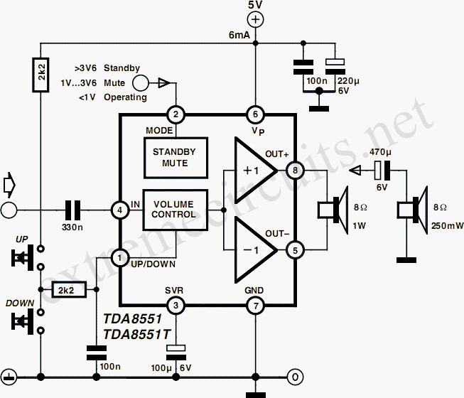 When
the power is switched on, the internal counter takes on the –20 dB
setting. An additional input (MODE) allows the amplifier to be switched
from the operating state to the mute or standby state. If this input is
held at the earth level, the amplifier is operational. If +5 V is
applied to this pin, the TDA8551 enters the Standby mode, in which the
current consumption drops from the typical operational level of 6mA to
less than 10µA. Finally, the MODE input can be used as a mute input by
applying a voltage of 1 t0 3.6 V to this input. This voltage can be
provided by a connection to the SCR pin, which lies at half of the
operating voltage and to which a filter capacitor is connected.
When
the power is switched on, the internal counter takes on the –20 dB
setting. An additional input (MODE) allows the amplifier to be switched
from the operating state to the mute or standby state. If this input is
held at the earth level, the amplifier is operational. If +5 V is
applied to this pin, the TDA8551 enters the Standby mode, in which the
current consumption drops from the typical operational level of 6mA to
less than 10µA. Finally, the MODE input can be used as a mute input by
applying a voltage of 1 t0 3.6 V to this input. This voltage can be
provided by a connection to the SCR pin, which lies at half of the
operating voltage and to which a filter capacitor is connected.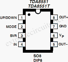 The
loudspeaker is connected in a floating configuration between the two
outputs of the bridge amplifier in the TDA8551. This provides the
desired output power level, in spite of the low supply voltage. For
headphone applications, which do not need as much output power, you can
connect the headphone between earth and one of the outputs, via an
electrolytic coupling capacitor. You can make a stereo headphone
amplifier in this way, using two TDS8551 ICs. The TDA8551 is housed in a
DIP8 package. The SMD version is the TDA8551T, in an SO8 package.
The
loudspeaker is connected in a floating configuration between the two
outputs of the bridge amplifier in the TDA8551. This provides the
desired output power level, in spite of the low supply voltage. For
headphone applications, which do not need as much output power, you can
connect the headphone between earth and one of the outputs, via an
electrolytic coupling capacitor. You can make a stereo headphone
amplifier in this way, using two TDS8551 ICs. The TDA8551 is housed in a
DIP8 package. The SMD version is the TDA8551T, in an SO8 package.