Friday 28 February 2014

Hi-Fi AUDIO POWER AMPLIFIERS


Small stereo amplifier project for computer

you want will build a Small stereo amplifier project for computer. This projects is best for you. Before read detail of they we should read mono model on This is Super Small Power Amplifier BCL 1.2W by TDA7052. If you are seeking the circuit amplifies small-sized. I begs for to advise this circuit because tiny economize with the equipment is a little.
This is Super Small Power Amplifier BCL 1.2W by TDA7052. If you are seeking the circuit amplifies small-sized. I begs for to advise this circuit because tiny economize with the equipment is a little. And still can use force against large-sized get comfortablely ( I has tried already ) besides it still use volt power supply very wide be about 1.5V arrive at 15V as well. Regard as IC TDA7052 be worthwhile very much. For you who want to try build this circuit. I has model PCB give a friend tests to see with. Request have fun the circuit amplifies miniature please.
 Power Amplifier Super Small BCL 1.2W by IC TDA7052
Circuit of Power Amplifier Super Small BCL 1.2W by IC TDA7052

PCB Power Amplifier Super Small BCL 1.2W by IC TDA7052


TDA 2050 Aamplifier

 
If you want to build hi-fi power amplifier the size about 30watt to 50Watt at good sound and build easy. I begs for to advise the circuit that builds with the integrated circuit. You wares IC TDA2050 then like very the circuit model class AB audio amplifier.
Thanks to its high power capability the TDA2050 is able to provide up to
35W true rms power into speaker 4 ohm load at THD =10%, VS =±18V, f = 1KHz and up to 32W into
8ohm load @THD = 10%, VS = 22V, f = 1KHz.Moreover, the TDA 2050 delivers typically 50W
music power into 4 ohm load over 1 sec at VS=22.5V, f = 1KHz
May take an interest want to try build already, try out this circuit use voltage Vcc +/- 25V.

Part
C1-0,47-22mF
C2-22mF
C3C4-100nF
C5-100(150)nF
R1R3-47kO
R2-1-3,3kO
R4-1-4,7oM/0,25W
Rt-4oM

PCB : 35W Hi-Fi AUDIO POWER AMPLIFIER by TDA2050

on PCB : 35W Hi-Fi AUDIO POWER AMPLIFIER by TDA2050


Mini 40 watt audio car amplifiers using HA13001

From this 20watt Integrated Amplifier project. Some people say that expensive and want the main amplifier only. I recommend this project, it had a budget of only 5$. and is the main amplifier. They have size of power to speaker is 40 watts and use voltage of power supply is 12 volts so can apply right in car. They use the HA13001-IC is key parts so small and build easily.
How This Circuit works
When see a circuit as Figure 1 Many people would doubt that. This circuit will be amplified up to 40 watts. (If as the RMS will is about 17.5 watts at load 4 ohms). You do not insult it because the many circuits that were contained in IC1-HA13001 of Hitachi there. Makes a few external devices, and the output of IC1 that connects to the loud speaker will be connected on the bridge circuit types. So causes the output has a high power there.
mini-40-watt-audio-car-amplifiers-using-ha13001
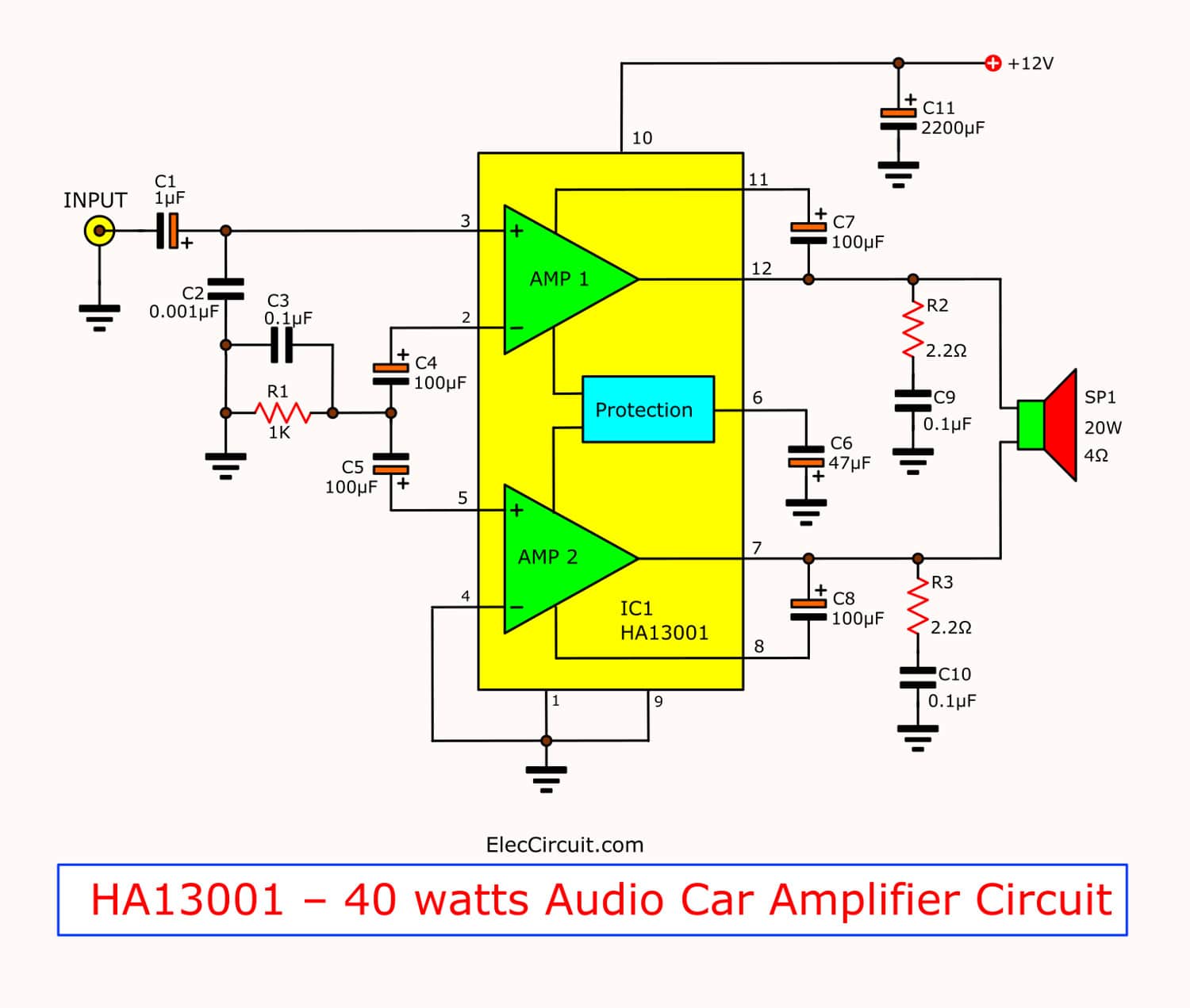
Figure 1 the circuits use IC-HA13001
We do not fear that the speaker will be damaged easily. because in IC1 has the Automatic Shut-Off circuit (ASO) that use to protect the speaker. Thus You need to carefree it. and this circuit will use the power supply range between about 12-18 volts for its’ source.
How to builds this projects
This simple project starting with make the PCB which has copper layout as figure 2 before. Then solder all components as figure 3. We can solder directly the IC1 onto PCB so should take special care.
pcb-of-mini-40-watt-audio-car-amplifiers
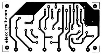
Figure 2 The PCB layout
the-components-layout-for-pcb-of-the-mini-40-watt-amplifiers
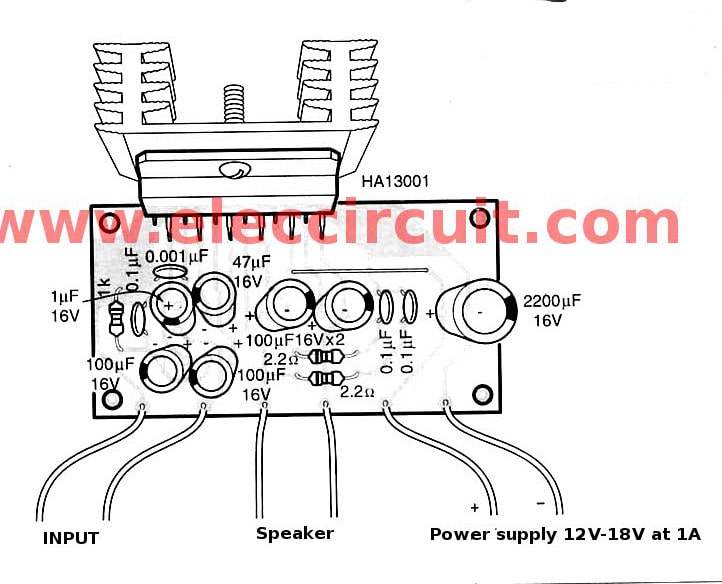
Figure 3 The components layout for PCB
The power supply that can use a DC adapter but must provide current over up 1 amperes. Otherwise, when you accelerate the more volume, the sound will be broken and Adapter will malfunction.
The application this projects
This amplifier project use to amplify from the various sound generator such as The iPad or mobile phone or notebook computer’s etc. Or Modified into the old car stereo that repair difficult. We changed the set to the amplifier.
The detial parts.
The electrolytic capacitors 16 volts
C1_________________1uF
C4, C5, C7, C8_______100uF
C6_________________47uF
C11________________2,200uF
The ceramic capacitors 50V
C2_________________0.001uF
C3, C9, C10__________0.1uF

IC1_number__________HA13001
¼ W + 5% Resistors
R1__________________1K
R2, R3_______________2.2 ohms
Speaker 20 W 4 ohms
Heat sink for IC1

High Current Voltage Regulation

Voltage regulators are available as easy to use three terminal integrated circuits - one terminal for the input voltage, one for the output voltage, and one for the ground (0V). The most commonly used are from the 78XX series - 7812 for 12 Volts, and 7805 for 5 Volts etc. Also of particular use for renewable energy generators are very efficient low dropout regulators such as the LM2940 series - LM2940CT-12 for 12 Volt etc.

One common shortfall of these common regulators is they are rated at just 1 Amp output current. It is usually possible to use them with higher currents, but a large heatsink and/or fan is essential. Regulators for higher currents than 1 Amp are available, but tend to be expensive, and still require good heatsinking.

Power transistor used with an LM78XX voltage regulator for high currents

Pictured above is a circuit from the Fairchild LM7812 datasheet. This uses a power transistor and a power resistor to take on some of the workload enabling higher currents to be regulated. With this set up, the power transistor and power resistor need heatsinking, and selecting the correct specification of transistor and resistor, and getting everything set up is not particularly easy.

One alternative is instead to parallel connect multiple three terminal regulators, with each regulator handling up to 1 Amp of current.

Parallel Connecting Mulitple Voltage Regulators

Voltage regulators such as the LM7812 cannot just be connected in parallel without additional circuitry. Each voltage regulator, though nominally rated at the same voltage, will in practice output a slightly different voltage - for example, three LM7812's could output 11.98, 12.01, and 12.06 respectively.

This tiny difference in voltage has the disastrous consequence of making the regulator with the lowest output voltage trying to carry all of the current. This will cause it's internal thermal protection to trigger (as the regulator overheats) effectively removing that regulator from the circuit and kicking off a chain reaction up through the remaining parallel-connected regulators.

Two LM7812 voltage regulators connected in parallel for a maximum output current of 2 Amp

The circuit shown above* (from the EDN article High-Current Supply uses Standard Three-terminal Regulator) has two LM7812 voltage regulators connected in parallel for a maximum total output current of 2 Amps - double the rated current of one LM7812.
* Diodes D1, D2, and D should be 1N4007 according to the EDN article, but common 1N4001 diodes will be fine as they are rated up to 50V which is more than enough. The capacitors are supposed to be C=47,000uF, C1 and C2 are 4,700uF, but as a 47,000uF capactitor is expensive and physically very large we tested this regulator using a 4,700uF for C, and 1,000uF for C1 and C2 and had no problems.

An even simpler way to parallel connect multiple voltage regulators together is to add very low (below 1 Ohm) ballast/equalising resistors in series with the regulator outputs. Doing so should make the regulators share current equally and therefore operate together without problems. It is worth noting however that this approach to load balancing makes the voltage regulation a bit less accurate.

Connecting 7812's in parallel with load balancing 0.25 Ohm resistors series connected to the outputs - 6 Amp 12 V regulated.

An example of this simplistic approach in use can be seen in the above experimental 12V 6A power supply* in which six LM7812 regulators were connected in parallel with 0.25 Ohm load balancing resistors (made up of four 1 Ohm resistors in parallel) connected in series with the output from each 7812 regulator. The schematic shows the key elements in this 6 Amp 12 Volt regulator.
* The original circuit diagram was published on the Wroclaw University of Technology website back when we first published this article in 2006/7. Unfortunately that article is no longer online.

High Current Variable Voltage Regulation

Where you need to have a user variable voltage output, the LM317 is an excellent adjustable voltage regulator to use. The output voltage is adjusted using a couple of resistors, and one of these resistors can be replaced with a potentiometer to give an adjustable output.

Adjustable high current power supply with LM317 voltage regulator


While the LM317T for example is limited to a continuous output of 1-1.5A subject to sufficient heatsinking, one or more power transistors can be added as shown above to make an adjustable high current power supply. Click here for full details: LM317 Adjustable Power Supply.


Comment on this Article

If you have any comments on this article, please email them to neil@reuk.co.uk.

Hello from Kentucky USA!

In regard to this page, I have drawn up a couple of 78xx high current circuits you might like to consider. I've used them for a 30amp power supply with a 7815 regulator.

Current regulation with a 78xx regulator


High current regulator using 78xx regulator and MJE3055 NPN transistors

REUK Added Info: The MJE3055 is an NPN silicon power transistor rated at up to 60V, up to 75 Watts, and up to 10 Amps. Click here to view the MJE3055 Datasheet for more information.
If you are unable to find the MJE3055, any NPN power transistor with a similar rating can be used instead. Click here to view a selection of NPN power transistors.


I have since switched to using the better LM723 regulator so that I can adjust the voltage and it is far more reliable than the 78xx. I have used the LM723 for a 105amp supply.

REUK Added Info:The LM723 is a voltage regulator rated for outputs of 150mA at an adjustable voltage from 2V to 37V. By adding transistors as shown in the schematics above high output currents at the regulated voltage can be output. Click here to view the LM723 datasheet.
The LM723 is available in the UK from around 30 pence. Click here to buy an LM723 now.


I've learned a few things on your site so I thought I'd pass along a little in return.

Ken Weaver, 17th August 2009


The benefit of this first schematic is that the output is actually regulated; the PNP is fully in the feedback loop.
However in Ken's circuit, the bases of the 3055 are regulated, but not the emitters, where the output is taken. Thus for every current ratio of 2.7 the voltage drops by 25mV.

Nick, 10th July 2012
rrent.

Monday 17 February 2014

Adjustable Power Supply with Charger

Circuit :
Notes:

This power supply has adjustable and charger output. The charger circuit can be use for cellular phone. The adjustable output serves as multipurpose power supply. It can handle a 1 ampere current. The 317 must have a heat sink.

PCB Layout:

Parts List:

Semiconductor:
LM 317 - 1pc
LED - 1pc
1N 4001 - 8pcs

Capacitors:
25V/470uF - 1pc
25V/10 uF - 1pc

Resistors:
1k, 1/2W - 1pc
220R, 1/2W - 1pc
5kR Potentiometer - 1pc

Others:
1Ampere, Multi-tap Transformer - 1pc
AC Chord - 1pc
Casing - 1pc
#22 Stranded Wire - 3m
Heatsink for TO220


Nicad Battery Charger


Description:

A basic nicad battery charger using a single medium power transistor.

Notes:

This simple charger uses a single transistor as a constant current source. The voltage across the pair of 1N4148 diodes biases the base of the BD140 medium power transistor. The base-emitter voltage of the transistor and the forward voltage drop across the diodes are relatively stable. The charging current is approximately 15mA or 45mA with the switch closed. This suits most 1.5V and 9V rechargeable batteries. The transformer should have a secondary rating of 12V ac at 0.5amp, the primary should be 220/240volts for Europe or 120volts ac for North America.

Warning:

Please take care with this circuit. Use a voltmeter to observe correct polarity. Nicads can explode if short circuited or connected with the wrong polarity.


Tuesday 11 February 2014

2WATTS FM TRANSMITTER

USE DIPOLE ANTENNA FOR MAXIMUM RANGE (COULD BE UP TO 10 KM IN GOOD WEATHER). TUNE BETWEEN 88-108 MHz WITH C5. BB-204 COULD BE REPLACED WITH CONVENTIONAL LED (BIG) WITH REVERSE BIAS (NO LIGHT GIVEN IN CORRECT POLARITY). 9V POWER FOR 2KM WITH GOOD SOUND QUALITY AND GRADUALLY UP TO 18V FOR 10 KM RANGE WITH POOR QUALITY OF SOUND.  BEST OF LUCK.


High Voltage Converter: 90V From 1.5V

The circuit shows one way of obtaining a voltage of 90V from a 1.5V battery supply. The LT1073 switching regulator from Linear Technology (http://www.linear-tech.com) operates in boost mode and can work with an input voltage as low as 1.0 V. The switching transistor, which is hidden behind connections SW1 and SW2, briefly takes one end of choke L1 to ground. A magnetic field builds up in the choke, which collapses when the transistor stops conducting: this produces a current in diode D1 which charges C3. The diode cascade comprising D1, D2, D3, C2, C3 and C4 multiplies the output voltage of the regulator by four, the pumping of C2 causing the voltage developed across C4 via C3, D2 and D3 to rise.


Finally, the regulator control loop is closed via the potential divider (10 MΩ and 24 kΩ). These resistors should be 1 % tolerance metal film types. With the given component values, fast diodes with a reverse voltage of 200 V (for example type MUR120 from On Semiconductor http://www.onsemi.com) and a choke such as the Coilcraft DO1608C-154 (http://www.coilcraft.com) an output voltage of 90 V will be obtained. The output of the circuit can deliver a few milliamps of current.

Build-very-low-cost-FM-transmitter

1. No. of stage: 4
2. Frequency of operation: About 100MHz
3. Antenna type: Folded 300 ohms dipole.
4. Range obtained in free space: Up to 4km with dipole antenna 30 feet above ground level. More   range with yagi antenna.


Brief Description:
The transmitter is built on a Printed Circuit Board. This board uses track inductor for L1, L2 and part of L3. The section built around Q1 is the oscillator section. Oscillation frequency is determined by L1, C4 & C5 which forms the tank. Actually C5 is the feedback capacitor. This is required to sustain oscillation. This also influence the operation of tank formed by L1 & C4. Modulation is directly applied to the base of Q1 via C2. A microphone is connected here to serve this purpose. You can alternately feed direct audio here after disconnecting the microphone biasing resistor R1. Q2, Q3 & Q4 gradually raises the output power up to the desired level.
As most of the inductors are PCB etched, there is practically very little frequency drift provided you use a highly regulated and ripple free power supply.
RF output from the transmitter is taken from the junction of C11 & C12. This is unbalanced output of around 75 ohms impedance. But a folded dipole is a balanced type antenna of around 300 ohms impedance. So we need to use a 'BALanced to UNbalanced transformer' or 'BALUN'. A 1:4 type BALUN is employed here for this purpose. Antenna connection is taken from this BALUN via a 300 ohms flat parallel feeder cable commonly used in television to receive terrestrial broadcast. No coaxia is used to feed antenna. This saves cost. Also a parallel feeder cable provides much less signal loss compared to a coaxial.
Design of BALUN
The BALUN is made using a two-hole binocular ferrite bead as shown above. You need to use parallel insulated twin wire to construct this. This wire is commonly used to wind TV BALUN transformer. If you want to get rid of this, then buy a ready-made TV BALUN that is generally used at the back of your television set for interfacing with feeder wire.  
 
If you prefer to build this yourself, the circuit diagram is given above. You need to carefully construct it keeping in mind about the 'sense' & 'direction' of turns. See there are four coils. Two coils in the upper section, which are red and blue, required to be wound on left side of the BALUN and the remaining two (blue & red) in the lower half to be wound on right side. Connection marked 'A' and 'B' at the left side of the circuit is reqired to be connected to the PCB at the shown point. As dipole antenna is balanced type, so you need not to worry about its connection.
 
PCB design details
The transmitter is built on a single sided PCB. As mentioned earlier, this PCB has a number of etched inductors. For this reason, you need to very carefully construct the PCB as mentioned below.


In the copper side view, you can see that there are three track etched inductors that resembles 'RCL' Every corner and track width/length are calculated and then they are drawn so that each 'RCL' section becomes an inductor of required value. Never play with this; otherwise, optimum result could not be achieved.
You need to use a laser printer or a high quality printer to get a printout of the drawings. First, save the picture to disk. Now try to print it from such a software which permits you to control print size. 'Paint Shop Pro' is such a software. Of course you can use any other software. Print the drawing so that copper side drawing is exactly 59mm X 59mm. Few trial will give you the perfect print. Now construct the PCB using 'Photo-etching' method so that all the tracks becomes exactly same as you are now seeing. Now drill the PCB carefully. The PCB is now ready to populate.
Start population according to the component mounting plan. You can also get a true size copy of this plan printed and glued to the PCB. This will help you work fast.Part of L3 is required to be constructed. This is described in parts list.
Please note that in the picture of the transmitter kit, capacitor C1 & C10 are not mounted by mistake and the kit is filmed. Please add these two capacitors. Try to keep all component leads as short as possible.
Now you need to design the dipole antenna to use with the kit.

N.B: Believe it or not, a 2N2369 from Philips, used in the final power amplifier section, can give this much of range. 


Detailed Parts List:

RESISTORS
R1 - 22K
R2 - 100K
R3, R7, R9 - 1K
R4, R8 - 100E
R5 - 390E
R6 - 330E
R10 - 15E
R11 - 10K
CAPACITORS
C1, C3, C10 - 1n
C2 - 100n
C4,C8,C9 - 47pF
C5, C11 - 10pF
C6 - 100uF/25V Electrolytic
C7 - 100pF
C12 - 3pF
TRANSISTORS
Q1, Q2, Q3 - BC548
Q4 - PN2369 (Plastic casing) or 2N2369 (Metal casing)
MISC.
L3 - 7 turns, 22SWG wire, 3mm ID, Close wound, Air core.
Two hole binocular BALUN core, BALUN wire, 300 ohms TV feeder wire,
JP1 to JP5 - All jumper wires.
This completes the Project. Please mail me with your feedback. It will really encourage me to give you more & more project like this.

Monday 10 February 2014

Battery charge controller

A charge controller circuit for battery makes you hassle-free by not bothering about switching the charger with different battery levels, the main advantages being improved life and low current consumption as it switches off the charger when battery full charged. So far we have published a simple battery charge controller circuit using 555 IC where many of our readers commented that it was difficult for them to set the threshold levels and also it seemed like it was harder to analyze working of the same.
For the above reasons, I have decided to introduce another one where you could find it easier to set the threshold levels. Furthermore, this charge controller design makes it easier for debugging. The main component of this circuit is a LM324 comparator IC which has four inbuilt comparators inside; here we are making use of only one. You can use any other comparator ICs instead of this one, like LM358, LM317, LM339 etc. I have used lm324 here owing to its high availability. For basic electronics learners see what is a comparator.
Read: Battery charging circuit with battery level indicator
As the threshold levels to turn ON and turn OFF the charger are different (hysteresis), it helps to avoid oscillation problems of the relay due to leakage current of battery. The threshold levels can be set by varying the potentiometer. As we are switching the charger with the help of relays, you can connect any capacity battery. High current transformers are recommended when using higher capacity batteries to decrease the charging time. For small capacity batteries you should use a series resistance to limit the charging current and that’s not necessary for higher capacity batteries.
This charging controller circuit can be applied with any system that makes use of rechargeable batteries like emergency, UPS, inverters, telephone receivers etc. Here we have used LEDs to indicate the charging status. Also at the bottom I have uploaded a video demonstration to guarantee you that this charge controller schematic is 100% working.

Battery charge controller circuit diagram

Components Required:

  1. LM324 IC
  2. Zener diode 5.1V
  3. Bridge IC/1N4007X4
  4. Transistor BC548X2
  5. Led Green
  6. Capacitor 1000uF
  7. Resistor 1KX4, 100K
  8. Pot 50K/47K
  9. Relay 12V/10A
  10. Transformer 0-15V/2A

Working:

  • Step down transformer steps down the line voltage to 15 volts and bridge rectifier does the AC to DC conversion process (rectification), it’s followed by the capacitor filter which removes AC ripples.
  • The power supply for the working of charger circuit is given from the battery (as it should always be monitoring the battery voltage level even when the mains supply is disconnected).
  • The non-inverting terminal of the comparator is connected to a zener diode and 1k resistor which are used to make a reference voltage of 5.1 volt, and its inverting terminal is used to monitor the battery level.
  • Usage of zener diode instead of resistors makes sure that the reference value is independent of battery level and temperature variances.
  • In fact the comparison is not between reference voltage and the actual battery voltage, but between a proportional value of battery level and reference value. This proportional value is achieved by using a potentiometer.
  • If the battery level is below the Lower Threshold Point (say LTP), then the reference voltage becomes higher than the proportional battery value. Thus output of comparator becomes positive.
  • Then the transistor is switched ON (as output of comparator is connected to the base of transistor BC548 through a 1k resistor) followed by the relay. I have used a freewheeling diode along with the relay to de-energize the inductor.
See:Working of relay with animation
  • And when the comparison goes reverse, output of comparator is low and transistors are OFF resulting in the disconnection of supply.
  • Output of comparator is also connected to another BC548 through a 1k resistor which make hysteresis. That means when the charger is ON, transistor is ON and it makes a 100k resistor parallel with the respective voltage divider, then the drop across the divider will again decrease increasing the charging level.
  • Upper Threshold Point (voltage level when charger is switched OFF) can be set by varying the potentiometer.
  • The difference between UTP and LTP (hysteresis) can be varied by changing the 100k resistor, decreasing the resistance increases the hysteresis and vice versa.
  • A 8.2ohm 10 watt resistor connected in series with the circuit helps to limit the charging current. It’s not required for higher capacity batteries as the charging time will increase.


IR Remote Switch Circuit


This circuit lets you control any line powered electrical device (a lamp, television, fan, etc.) using any infra-red remote control. Almost everyone these days has a pile of old IR remotes left over from appliances they have long ago disposed of them. With this circuit, you can put them back into use. The circuit looks for any modulated IR source and uses it to control a TRIAC, which then switches any appliance connected to it's socket. For example, you can use it to control the room lighting in your home theater setup using any of the remotes you already have. The circuit is powered using a simple transformer less power supply from the line itself, making it compact and easily built into a light switch, wall box, power bar or even the appliance you wish to control. Schematic


Part
Total Qty.
Description
R1
1
3 Meg 1/4W Resistor
R2
1
1.2 Meg 1/4W Resistor
R3
1
680 Ohm 1/4W Resistor
R4
1
2K 1/4W Resistor
R5
1
4.7K 1/4W Resistor
R6
1
150 Ohm 1/4W Resistor
C1
1
0.001uF Ceramic Disc Capacitor
C2, C5
2
1uF 50V Tantalum Electrolytic Capacitor
C3
1
47uF 50V Tantalum Electrolytic Capacitor
C4
1
10uF 50V Tantalum Electrolytic Capacitor
C5
1
150 Ohm 1/4W Resistor
D1
1
1N4733 5V Zener Diode
D2
1
1N4003 Rectifier Diode
Q1
1
2N6071A TRIAC
U1
1
GP1U52X IR Module
U2
1
MC74HC74 D-Type Flip Flop
U3
1
MOC3011 Opto Isolator
MISC
1
Board, Sockets For ICs, Mains Socket, Mains Plug and Cord, Wire
 
  1. Under normal circumstances, Q1 should not need a heatsink.
  2. The circuit is designed for a supply voltage of 120V.
  3. The printed circuit pattern is reproduced here larger then real life for clarity. It will need to be resized to the scale at the bottom of the image if you intend to transfer it to a board.
The circuit functions as an on/off flip flop. Illuminate it with your remote once to turn it on, then again to turn it off.